Computer ARchitecture &
Embedded Systems Laboratory
 > Research Area > Flash Memory System
1. An FPGA-based development platform for SSD
- Designed as an open framework for designing, implementing, and evaluating HW/SW components for SSDs
- Delivering performance comparable to commercially available SSDs
2. BlueSSD hardware
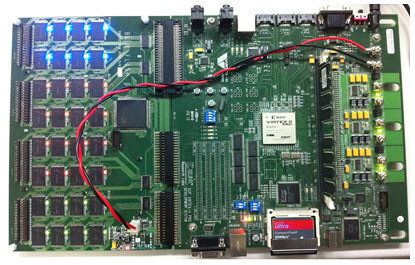
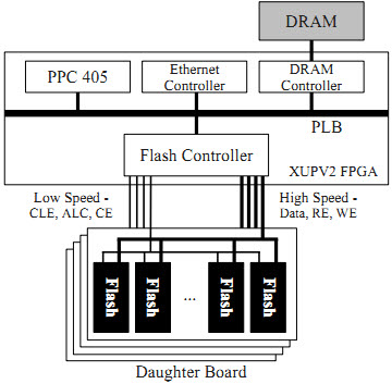
- Built on top of the Xilinx XUPV2P FPGA board and the custom flash storage daughter board which holds up to 8 packages and up to 16 chip-enables.
- Populated with 32 1GB MLC flash parts, each with a single chip enable.
- PowerPC 405 on the XUP board runs the Linux 2.6.25.3 kernel that is used as a platform for firmware such as a flash translation layer.

3. BlueSSD software
- Provide a flexible software infrastructure so that several flash management schemes can be employed with minimal modifications to the existing software system.
- Overall structure of the flash firmware, which is composed of 3 layers: a device driver for the flash controller, a host interface, and a flash translation layer.


4. Published papers
Sungjin Lee, Kermin Fleming, Jihoon Park, Keonsoo Ha, Adrian Caulfield, Steven Swanson, Arvind, and Jihong Kim, "BlueSSD: An Open Platform for Cross-layer Experiments for NAND Flash-based SSDs," International Workshop on Architectural Research Prototyping (WARP '10) in conjunction with ISCA 2010, Saint-Malo, France, June 19, 2010
Sungjin Lee, Jihoon Park, Kermin Fleming, Arvind, and Jihong Kim, "Improving Performance and Lifetime of Solid-State Drives Using Hardware-Accelerated Compression," IEEE Transactions on Consumer Electronics, Vol. 57, Issue 4, pp. 1732-1739, December 2011
Sungjin Lee, Jisung Park, and Jihong Kim, "FlashBench: A Workbench for a Rapid Development of Flash-Based Storage Devices," To be presented at International Symposium on Rapid System Prototyping (RSP'12) in conjunction with ESWEEK 2012, Tampere, Finland, October 11-12, 2012